歡迎您,浏覽北京金池廣信科技有限公司官方網站(zhàn)!
服務熱線:+86-10-53821869 / +86-755-23480857

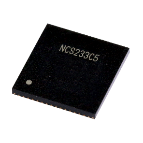
NCS233C5
- 輸入類型 : XTAL, Single-Ended,Differential-Ended inputs
- 輸入端口數 : 5
- 輸出端口數 : 12
- 輸出類型 : LVDS, LVPECL, LVCMOS,HCSL
- 器件類型 : Network Synchronization PLL
- Core Supply Voltage(V) :
- Output Supply Voltage(V) :
- Output frequency(Min)(MHz) :
- Output frequency(Max)(MHz) :
- Additive Jitter(fs) :
- Temperature Range :
- Package :
輸入端口數: 5
輸出端口數: 12
輸出類型: LVDS, LVPECL, LVCMOS,HCSL
器件類型: Network Synchronization PLL
産品描述
NCS233C5 is a programmable loop bandwidth Network Synchronization PLL that provides jitter attenuator function and synchronization clock function for many systems. All PLL components are fully integrated on-chip, eliminating the risk of noise coupling associated with discrete solutions. It features 5 differential or single-ended clock inputs and 12 differential or 24 single-ended clock outputs. Furthermore, 4 independent APLL/ DPLL outputs can be locked to any of the inputs and sent to any of the chip outputs. Each output can be configured as LVDS, LVPECL or two single-ended LVCMOS. In addition, each output clock phase can be adjusted dynamically. NCS233C5 supports free-run, synchronous and holdover modes as well as enhanced automatic or manual hitless switching between input clocks. It is programmable by I2C or SPI serial interface. NCS233C5 is capable of generating any combination of output frequency from any input frequency as specified in the datasheet.
産品參數
• Generate any combination of output frequencies from any input frequency
• External XTAL or XO reference frequency from 10MHz to 285MHz
• Ultra-low phase jitter of 140 fs RMS 12kHz- 20MHz
• Supports free-run, synchronous (Lock input) and holdover modes as well as enhanced hitless switching
• Supports up to 4 independent APLL/DPLL loops and 12 outputs
• Supports 4 differential or single-ended clock inputs
• Meets G.8262, G.8262.1 EEC Standards
• Status monitoring (LOS, OOF, LOL)
• Zero delay mode
• DCO mode
• Supports 1PPS input/SyncE/IEEE1588
• Supports JESD204B/C
• Duty Cycle Modulation
• TDC
• Serial Interface: I2C or SPI
• Input frequency range
Differential: 0.5 Hz to 1 GHz
LVCMOS: 0.5 Hz to 250 MHz
• Output frequency range
Differential: 0.5 Hz to 1.5 GHz
LVCMOS: 0.5 Hz to 250 MHz
• Highly configurable outputs format
compatible with LVDS, LVPECL, LVCMOS, CML and HCSL with programmable signal
amplitude and output common voltage
• Independent output clock supply pins: 3.3V, 2.5V, or 1.8V.
相關産品
産品咨詢
北京總公司
北京市朝陽區(qū)望京綠地中心A座A區(qū)9層
電話(huà):+86-10-53821869
深圳子公司
↵廣東省深圳市福田區(qū)深南大(dà)道(dào)6019号金(jīn)潤大(dà)廈8層
電話(huà):+86-755-23480857
西安分公司
西安市高(gāo)新區(qū)錦業一路52号寶德雲谷國際B座2003
電話(huà):+86-29-81128637
合肥子公司
↵合肥市高(gāo)新區(qū)創新大(dà)道(dào)2800号創新産業園2期F棟705
電話(huà):+86-551-63657380


